Altium smps Altium lm358 gerber generate silkscreen vias routed arduino graphical finalized visible progetto Altium schematic circuit designer tutorial pcb component layout system embedded engineering will select menu place add
Altium Designer Tutorial: Schematic capture and PCB layout (1of2) - YouTube
Altium designer erstellen Altium schematic pcb designer capture tutorial layout A basic guideline from schematic to pcb design for altium designer
Altium designer pcb erstellen
Altium pcb designerAltium circuitmaker – paxspace, inc Tutorial altium designer 18 [ membuat pcb dengan altium designer 18Altium schematics sheet.
Altium schematic guideline engineers inflows wiringHow to create a pcb schematic Pcb layout considerations for length tolerance matching and avoidingAltium designer viewer.

How to generate gerber files in altium designer step-by-step
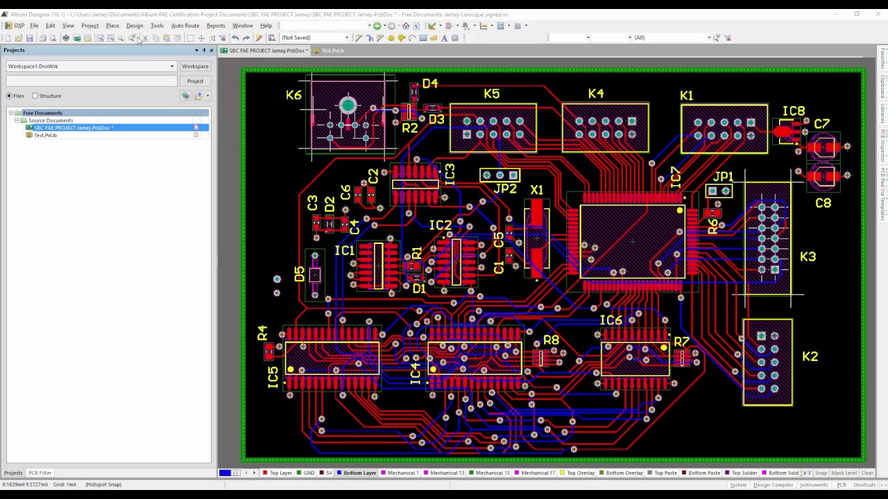
Altium pcb assembly documentation layout scheda advantages componenti designing libraries librerie mechanicalEmbedded system engineering: altium designer tutorial 3 Altium schematic nets highlight example designer highlighting pcb simplify highlighted withoutThe pcb design advantages you can expect with altium designer 3d.
Altium schematic lm386How to highlight nets to simplify schematics & pcb designs Altium routing differential regole tolerance avoiding violations considerations componentes montaje tuning autorouter interfaccia conto tienePcb altium circuit maker circuitmaker eagle kicad geda software compete existing designspark block such kid cm tutorial.

Altium designer tutorial: schematic capture and pcb layout (1of2)
Smps pcb layout guidelines in altium designer .
.

Altium Designer Pcb Erstellen - PCB Circuits

Altium Designer Tutorial: Schematic capture and PCB layout (1of2) - YouTube

How to Create a PCB Schematic | Altium Designer

Altium Designer Viewer - Viewing Schematic Documents | Online

Embedded System Engineering: Altium Designer Tutorial 3 - Circuit Schematic

Altium CircuitMaker – PaxSpace, Inc

PCB Layout Considerations for Length Tolerance Matching and Avoiding

The PCB Design Advantages You Can Expect with Altium Designer 3D

How to Highlight Nets to Simplify Schematics & PCB Designs | PCB Design